CORE EQUIP
核心设备集群
CORE EQUIPMENT
HARDWARE RESOURCES
HARDWARE RESOURCES
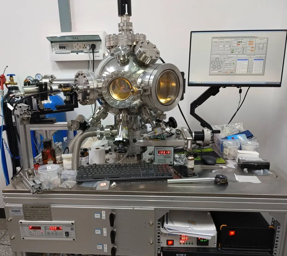
脉冲激光沉积系统
Pulsed Laser Deposition
PLD
利用高能量脉冲激光轰击靶材,用于高质量多铁性氧化物薄膜及超晶格的原子级外延生长。实验室共 3 套。
Utilizes high-energy pulsed laser ablation for atomic-level epitaxial growth of high-quality multiferroic oxide thin films and superlattices. Three systems are in service.
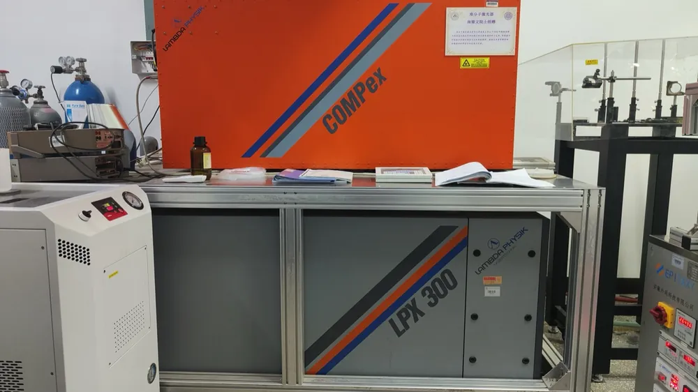
脉冲激光器
Pulsed Laser
Laser
配套 PLD 系统使用,提供薄膜沉积所需的高能量脉冲激光源。本设备由清华大学南策文院士捐赠。
Paired with the PLD system to provide the high-energy pulsed laser source for film deposition. Donated by Academician Ce-Wen Nan of Tsinghua University.
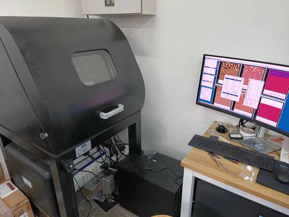
扫描探针显微镜
Scanning Probe Microscope
SPM/AFM
用于薄膜表面形貌(AFM)、压电响应(PFM)以及磁力显微镜(MFM)的高精度纳米级表征。
Used for high-precision nanoscale characterization of film surface topography (AFM), piezoresponse (PFM), and magnetic domain structures (MFM).
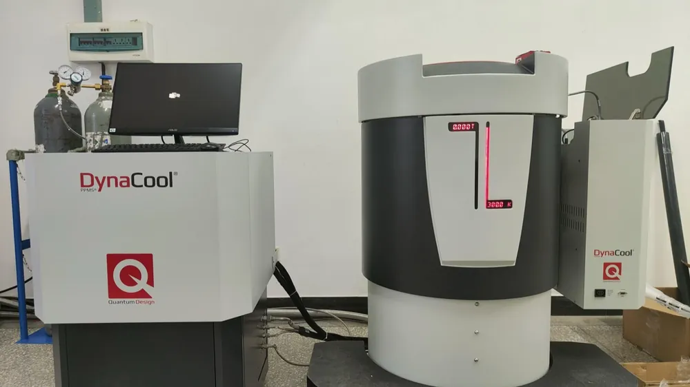
综合物理性质测量系统
Physical Property Measurement System
PPMS
提供极低温与强磁场环境,用于薄膜材料的电学、磁学及热学等精密综合物性测量。
Provides ultra-low temperature and high magnetic field environments for precise comprehensive measurements of electrical, magnetic, and thermal properties.
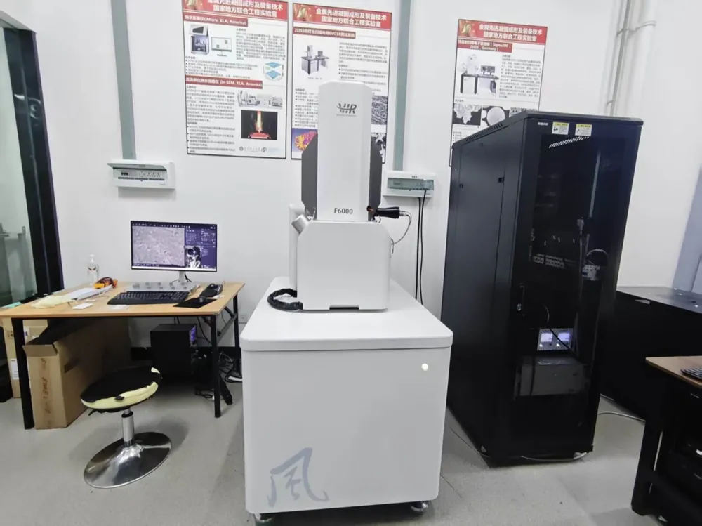
扫描电子显微镜
Scanning Electron Microscope
SEM
利用聚焦电子束扫描样品表面,观察薄膜与异质结的微观形貌、界面及成分分布。感谢惠然科技捐赠!
Images micro-morphology, interfaces, and elemental distribution of thin films and heterostructures via a focused electron beam. Donated by WellRun Technology.
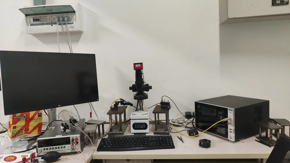
铁电测试仪
Ferroelectric Tester
FE Tester
测量铁电薄膜的电滞回线(P-E loop)、漏电流与疲劳特性,表征铁电极化行为。
Measures P-E hysteresis loops, leakage current, and fatigue characteristics to characterize ferroelectric polarization behavior.
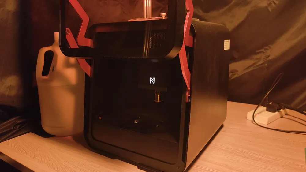
无掩膜紫外光刻机
Maskless UV Lithography System
UV Litho
基于无掩膜数字光刻技术,快速制备微纳图形电极与器件,支持柔性版图设计。
Digital maskless lithography for rapid fabrication of micro/nano-patterned electrodes and devices with flexible layout design.